- 您现在的位置:买卖IC网 > Sheet目录3881 > PIC18F8585T-I/PT (Microchip Technology)IC PIC MCU FLASH 24KX16 80TQFP
PIC18F6585/8585/6680/8680
DS30491C-page 128
2004 Microchip Technology Inc.
10.2
PORTB, TRISB and LATB
Registers
PORTB is an 8-bit wide, bidirectional port. The corre-
sponding data direction register is TRISB. Setting a
TRISB bit (= 1) will make the corresponding PORTB
pin an input (i.e., put the corresponding output driver in
a high-impedance mode). Clearing a TRISB bit (= 0)
will make the corresponding PORTB pin an output (i.e.,
put the contents of the output latch on the selected pin).
The Data Latch register (LATB) is also memory mapped.
Read-modify-write operations on the LATB register read
and write the latched output value for PORTB.
EXAMPLE 10-2:
INITIALIZING PORTB
Each of the PORTB pins has a weak internal pull-up. A
single control bit can turn on all the pull-ups. This is
performed by clearing bit RBPU (INTCON2<7>). The
weak pull-up is automatically turned off when the port
pin is configured as an output. The pull-ups are
disabled on a Power-on Reset.
Four of the PORTB pins (RB3:RB0) are the external
interrupt pins, INT3 through INT0. In order to use these
pins as external interrupts, the corresponding TRISB
bit must be set to ‘1’.
The other four PORTB pins (RB7:RB4) have an
interrupt-on-change feature. Only pins configured as
inputs can cause this interrupt to occur (i.e., any
RB7:RB4 pin configured as an output is excluded from
the interrupt-on-change comparison). The input pins (of
RB7:RB4) are compared with the old value latched on
the last read of PORTB. The “mismatch” outputs of
RB7:RB4 are OR’ed together to generate the RB port
change interrupt with flag bit, RBIF (INTCON<0>).
This interrupt can wake the device from Sleep. The
user, in the Interrupt Service Routine, can clear the
interrupt in the following manner:
a)
Any read or write of PORTB (except with the
MOVFF
instruction). This will end the mismatch
condition.
b)
Clear flag bit RBIF.
A mismatch condition will continue to set flag bit, RBIF.
Reading PORTB will end the mismatch condition and
allow flag bit RBIF to be cleared.
The interrupt-on-change feature is recommended for
wake-up on key depression operation and operations
where PORTB is only used for the interrupt-on-change
feature. Polling of PORTB is not recommended while
using the interrupt-on-change feature.
For PIC18FXX85 devices, RB3 can be configured by the
configuration bit, CCP2MX, as the alternate peripheral
pin for the CCP2 module. This is only available when the
device is configured in Microprocessor, Microprocessor
with Boot Block, or Extended Microcontroller Operating
modes.
The RB5 pin is used as the LVP programming pin.
When the LVP configuration bit is programmed, this pin
loses the I/O function and becomes a programming test
function.
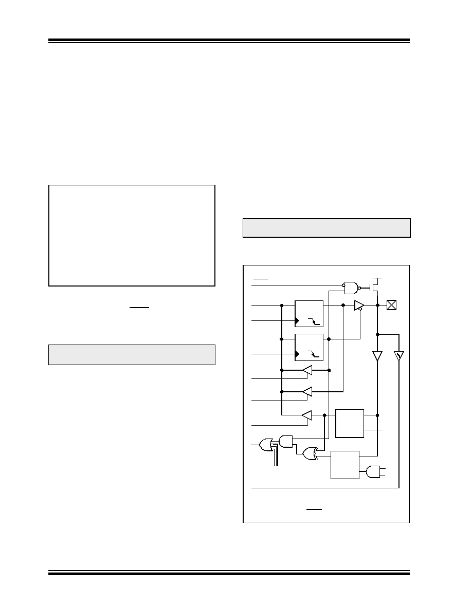
FIGURE 10-5:
BLOCK DIAGRAM OF
RB7:RB4 PINS
Note:
On a Power-on Reset, these pins are
configured as digital inputs.
CLRF
PORTB
; Initialize PORTB by
; clearing output
; data latches
CLRF
LATB
; Alternate method
; to clear output
; data latches
MOVLW
0CFh
; Value used to
; initialize data
; direction
MOVWF
TRISB
; Set RB<3:0> as inputs
; RB<5:4> as outputs
; RB<7:6> as inputs
Note:
When LVP is enabled, the weak pull-up on
RB5 is disabled.
Data Latch
From other
RBPU(2)
P
VDD
I/O pin(1)
Q
D
CK
Q
D
CK
QD
EN
QD
EN
Data Bus
WR LATB
WR TRISB
Set RBIF
TRIS Latch
RD TRISB
RD PORTB
RB7:RB4 pins
Weak
Pull-up
RD PORTB
Latch
TTL
Input
Buffer
ST
Buffer
RB7:RB5 in Serial Programming Mode
Q3
Q1
RD LATB
or PORTB
Note 1:
I/O pins have diode protection to VDD and VSS.
2:
To enable weak pull-ups, set the appropriate TRIS bit(s)
and clear the RBPU bit (INTCON2<7>).
发布紧急采购,3分钟左右您将得到回复。
相关PDF资料
XF2J-2424-11
CONN FPC 24POS 0.5MM SMT
PIC18LF6585T-I/PT
IC PIC MCU FLASH 24KX16 64TQFP
PIC18LF6680T-I/PT
IC PIC MCU FLASH 32KX16 64TQFP
XF2J-2224-11
CONN FPC 22POS 0.5MM SMT
PIC18F6525T-I/PT
IC PIC MCU FLASH 24KX16 64TQFP
PIC18F4439-E/ML
IC PIC MCU FLASH 6KX16 44QFN
XF2J-2024-11
CONN FPC 20POS 0.5MM SMT
PIC16LF747-I/ML
IC PIC MCU FLASH 4KX14 44QFN
相关代理商/技术参数
PIC18F85J10-I/PT
功能描述:8位微控制器 -MCU 32 KB FL 2 KB RAM RoHS:否 制造商:Silicon Labs 核心:8051 处理器系列:C8051F39x 数据总线宽度:8 bit 最大时钟频率:50 MHz 程序存储器大小:16 KB 数据 RAM 大小:1 KB 片上 ADC:Yes 工作电源电压:1.8 V to 3.6 V 工作温度范围:- 40 C to + 105 C 封装 / 箱体:QFN-20 安装风格:SMD/SMT
PIC18F85J10-I/PT
制造商:Microchip Technology Inc 功能描述:IC 8BIT MCU PIC18F 40MHZ TQFP-80 制造商:Microchip Technology Inc 功能描述:IC, 8BIT MCU, PIC18F, 40MHZ, TQFP-80
PIC18F85J10T-I/PT
功能描述:8位微控制器 -MCU 32 KB FL 2 KB RAM RoHS:否 制造商:Silicon Labs 核心:8051 处理器系列:C8051F39x 数据总线宽度:8 bit 最大时钟频率:50 MHz 程序存储器大小:16 KB 数据 RAM 大小:1 KB 片上 ADC:Yes 工作电源电压:1.8 V to 3.6 V 工作温度范围:- 40 C to + 105 C 封装 / 箱体:QFN-20 安装风格:SMD/SMT
PIC18F85J11-I/PT
功能描述:8位微控制器 -MCU 32KB Flash 2048BRAM 67I/O RoHS:否 制造商:Silicon Labs 核心:8051 处理器系列:C8051F39x 数据总线宽度:8 bit 最大时钟频率:50 MHz 程序存储器大小:16 KB 数据 RAM 大小:1 KB 片上 ADC:Yes 工作电源电压:1.8 V to 3.6 V 工作温度范围:- 40 C to + 105 C 封装 / 箱体:QFN-20 安装风格:SMD/SMT
PIC18F85J11T-I/PT
功能描述:8位微控制器 -MCU 32KB Flash 2048bytes-RAM 67I/O RoHS:否 制造商:Silicon Labs 核心:8051 处理器系列:C8051F39x 数据总线宽度:8 bit 最大时钟频率:50 MHz 程序存储器大小:16 KB 数据 RAM 大小:1 KB 片上 ADC:Yes 工作电源电压:1.8 V to 3.6 V 工作温度范围:- 40 C to + 105 C 封装 / 箱体:QFN-20 安装风格:SMD/SMT
PIC18F85J15-I/PT
功能描述:8位微控制器 -MCU 48 KB FL 4 KB RAM RoHS:否 制造商:Silicon Labs 核心:8051 处理器系列:C8051F39x 数据总线宽度:8 bit 最大时钟频率:50 MHz 程序存储器大小:16 KB 数据 RAM 大小:1 KB 片上 ADC:Yes 工作电源电压:1.8 V to 3.6 V 工作温度范围:- 40 C to + 105 C 封装 / 箱体:QFN-20 安装风格:SMD/SMT
PIC18F85J15T-I/PT
功能描述:8位微控制器 -MCU 48 KB FL 4 KB RAM RoHS:否 制造商:Silicon Labs 核心:8051 处理器系列:C8051F39x 数据总线宽度:8 bit 最大时钟频率:50 MHz 程序存储器大小:16 KB 数据 RAM 大小:1 KB 片上 ADC:Yes 工作电源电压:1.8 V to 3.6 V 工作温度范围:- 40 C to + 105 C 封装 / 箱体:QFN-20 安装风格:SMD/SMT
PIC18F85J50-I/PT
功能描述:8位微控制器 -MCU 32KB Flash 3936byte RAM RoHS:否 制造商:Silicon Labs 核心:8051 处理器系列:C8051F39x 数据总线宽度:8 bit 最大时钟频率:50 MHz 程序存储器大小:16 KB 数据 RAM 大小:1 KB 片上 ADC:Yes 工作电源电压:1.8 V to 3.6 V 工作温度范围:- 40 C to + 105 C 封装 / 箱体:QFN-20 安装风格:SMD/SMT